
Type
Video

Interface

Signaling
PCIe 1.0
PCIe 2.0
PCIe 3.0
PCIe 4.0
PCI ID
7360

RAM type
HBM2

RAM size
8 GB
| Board Design |
|---|
|
| Length |
|
| Slot Width |
Dual-slot
|
| Board Number |
109-D30587-00_05P
|
| Board Model Name |
Radeon Pro V520 / XFX BC-160 / JieShuo BC-160
|
| Board Manufacturer |
AMD / XFX / JieShuo
|
| Memory Configuration (Board Specific) |
|---|
|
| Memory Size |
8192 MB
|
| Memory Type |
GDDR6 controller bridge to HBM2 stacks
|
| Memory Brand |
Hynix
|
| Memory Model |
|
| Memory Bandwidth |
512 GB/s
|
| Release Information |
|---|
|
| Release Date |
Jun 15th, 2020
|
| Launch Price USD |
Not Applicable (Enterprise/OEM)
|
| Production Status |
EOL
|
| Product Generation |
Navi / RDNA 1.0
|
| Clock Speeds (Board Specific) |
|---|
|
| GPU Clock |
1000 MHz
|
| Boost Clock |
1600 MHz
|
| Memory Clock |
1000 MHz (HBM2) / 2000 MHz (GDDR6)
|
| Effective Memory Speed |
2.0 Gbps (HBM2) / 16 Gbps (GDDR6)
|
| Power and Thermal |
|---|
|
| Total Board Power |
~230 W
|
| Thermal Design Power TDP |
225 W
|
| Multi-GPU |
|---|
|
| Crossfire |
Untested
|
| Features and API support |
|---|
|
| WDDM |
3.0
|
| Shader ISA |
GFX 10.1 (gfx1011)
|
| System DMA |
5.0.5
|
| Shader Model |
6.0
|
| OpenCL Support |
2.2
|
| OpenGL Support |
4.6
|
| Vulkan Support |
1.3
|
| Display Core Next |
2.1.0
|
| Ray Tracing Cores |
No
|
| Graphics Controller |
10.1.2
|
| VIdeo Encode Engine |
VCN 2.0.2
|
| Video Decode Engine |
VCN 2.0.2
|
| DirectX Feature Level |
12 (12.1)
|
| Virtualization Support |
AMD MxGPU Technology (SR-IOV)
|
| Core Architecture |
|---|
|
| Foundry |
TSMC
|
| Die Size |
|
| GPU Name |
Navi 12
|
| Part Number |
215-0929036
|
| Transistors |
|
| Process Size |
7 nm
|
| Bus Interface |
PCI-e 4.0 x16
|
| Microarchitecture |
RDNA 1.0
|
| Cache Hierarchy |
|---|
|
| Shared L2 Cache |
4096 KB
|
| CU Vector Data Cache |
16 KB
|
| WGP Local Data Share |
128 KB
|
| WGP Instruction Cache |
32 KB
|
| SIMD32 Scalar Register File |
10 KB
|
| CU Local Data Share (GCN-Mode) |
64 KB
|
| WGP Scalar Data Cache / K Cache |
16 KB
|
| Core Configuration |
|---|
|
| DMA Engines |
1
|
| Compute Units |
36
|
| Hardware Schedulers |
1
|
| Async Compute Engines |
4
|
| Shading Units / Cores |
2304
|
| Render Output Units (ROPs) |
64
|
| Texture Mapping Units (TMUs) |
144
|
| Theoretical Performance |
|---|
|
| Pixel Rate |
102.4 GPixel/s
|
| Texture Rate |
230.4 GTexel/s
|
| FP16 (half) Performance |
14.75 TFLOPS (2:1)
|
| FP32 (float) Performance |
7.373 TFLOPS
|
| FP64 (double) Performance |
460.8 GFLOPS (1:16)
|
| Performance Calculation Notes |
Pixel Rate = ROPs * Boost Clock. Texel Rate = TMUs * Boost Clock. FP32 Performance = (Shading Units * Boost Clock * 2) / 1000.
|
| Memory Interface |
|---|
|
| Memory Bus |
256bit GDDR6
|
| Memory Bandwidth |
512 GB/s
|
| Memory Bus Bridge |
2048-bit (HBM2)
|
| Memory Controller Type |
GDDR6 bridged to HBM2
|
| Memory Clock on GDDR6 controller |
2000MHz
|
| Clock and Power |
|---|
|
| Core Clock |
1000 MHz
|
| Boost Clock |
1600 MHz
|
| TDP (Thermal Design Power) |
225 W
|

I/O ports

Power connectors
Last updated 2025-06-11T14:56:26Z
Disclaimer
The info found in this page might not be entirely correct. Check out this guide to learn how you can improve it.
 Image 1 of 4 (Rigo "0xCats" Reddig)
 Image 2 of 4 (Rigo "0xCats" Reddig)
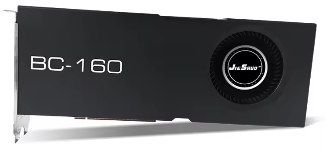 Image 3 of 4 (JieShuo)
 Image 4 of 4 (Rigo "0xCats" Reddig)