| Compute Architecture | |
|---|---|
| CPU Instruction Sets | AVX-512, AVX-VNNI |
| Integrated CPU Cores | 2x Intel Sunny Cove Cores |
| Primary Compute Units | 12 Inference Compute Engines (ICE) |
| ICE Compute Capability | 4K MAC/cycle per ICE (4D Grid: 32x32x4) |
| Integrated Vector Processor | Customized Tensilica Vision P6 DSP (512-bit vector width) |
| System Interface and Power | |
|---|---|
| Host Interface | PCIe 3.0 x8 (M.2 form factor only exposes x4) |
| Power Management | Fully Integrated Voltage Regulation (FIVR), DVFS |
| External Memory Controller | Quad-channel LPDDR4X-4266 |
| Thermal Design Power (TDP) | 12 W (configurable up to ~25 W) |
| External Memory ECC Support | Yes (Not Used) |
| On-Board Memory | |
|---|---|
| Brand | Micron |
| Model | MT53D1024M32D4DT-046 |
| Total RAM | 16GB |
| Configuration | 4x 32bit LPDDR4x |
| Architecture Identity | |
|---|---|
| Model | Intel Nervana NNP-I 1150 |
| Codename | Spring Hill |
| Process Technology | Intel 10nm FinFET CMOS |
| Primary Market Segment | Deep learning inference acceleration for data center and edge |
| On-Chip Memory Hierarchy | |
|---|---|
| Deep SRAM | 48 MiB Total (4 MiB per ICE) |
| On-Chip Communication | Integrated ring bus architecture |
| Last Level Cache (LLC) | 24 MiB Total (8 cache slices x 3 MiB) |
| Tightly-Coupled Memory (TCM) | 3 MiB Total (256 KiB per ICE) |
| Feature and Performance Summary | |
|---|---|
| Peak Performance | 50 TOPS (at INT8 precision) |
| Supported Data Types | INT8, FP16, 4-bit, 2-bit, 1-bit |
| Software Compatibility | TensorFlow, PyTorch, ONNX via nGraph |
| Compute Engines | |
|---|---|
| CPU L2 Cache | 512 KB per core |
| CPU Thread Count | 2 |
| CPU Instruction Sets | x86-64, AVX-512, AVX-VNNI |
| Integrated CPU Cores | 2x Intel Sunny Cove (IceLake) |
| Integrated Vector DSP | Cadence Tensilica Vision P6 (512-bit VLIW) |
| ICE Compute Capability | 4096 MACs per cycle |
| Inference Compute Engine (ICE) Count | 12 |
| Core Architecture | |
|---|---|
| Codename | Spring Hill |
| Die Size | 239 mm² |
| Chip Model | Nervana NNP-I 1150 |
| Transistor Count | 8.5 billion |
| Process Technology | Intel 10nm FinFET CMOS |
| On-Chip Interfaces | |
|---|---|
| Max Memory Bandwidth | 68.25 GB/s |
| Internal Interconnect | Integrated Ring Bus Architecture |
| Host Interface Controller | PCIe 3.0 x8 |
| External Memory Controller | Quad-channel LPDDR4X-4266 |
| On-Chip Memory Hierarchy | |
|---|---|
| Deep SRAM | 48 MiB Total (4 MiB per ICE) at ~6.8 TB/s |
| Last Level Cache (LLC) | 24 MiB Total (8 cache slices) at ~680 GB/s |
| Tightly-Coupled Memory (TCM) | 3 MiB Total (256 KiB per ICE) at ~68 TB/s |
| Power and Thermal | |
|---|---|
| TDP (Base) | 12 Watt |
| Power Management Technology | FIVR, DVFS |
| Chip-Level Features | |
|---|---|
| Peak Performance | 50 TOPS (INT8) |
| Supported Special Data Precisions | FP16, INT8, INT4, INT2, INT1 |
The Intel Nervana NNP-I 1150 (Spring Hill, SRK1U) is an M.2 Key M form factor inference accelerator. It integrates two Intel Sunny Cove cores and twelve Inference Compute Engines (ICEs) on a 10nm SoC. The chip includes 24 MB of shared LLC, 3 MB of tightly coupled memory (256 KB per ICE), and 48 MB of deep SRAM (4 MB per ICE). It supports LPDDR4x-4266 memory with 16 or 32 GB capacity and 67.2 GB/s bandwidth.
The card connects via M.2 PCIe Gen3 x4 and has a typical TDP of 12W. It is designed to accelerate low-latency AI inference workloads and operates independently with an embedded Linux-based OS loaded by the host driver at runtime.
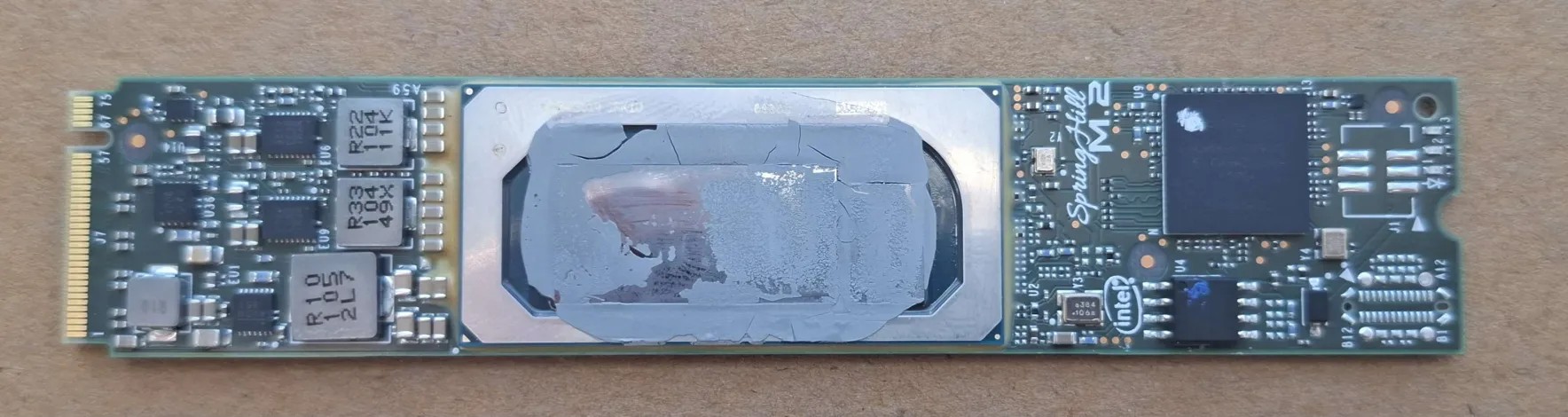 Image 1 of 3 (Rigo "0xCats" Reddig)
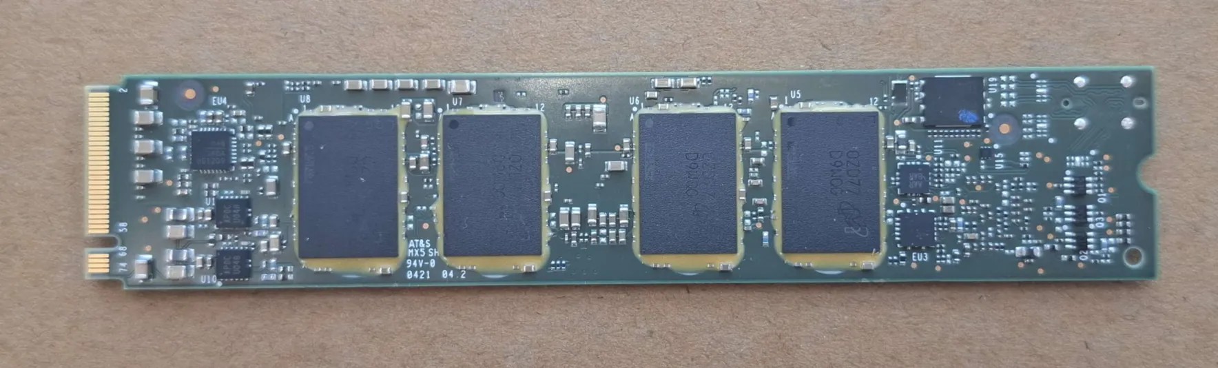 Image 2 of 3 (Rigo "0xCats" Reddig)
 Image 3 of 3 (Rigo "0xCats" Reddig)
Disclaimer
The info found in this page might not be entirely correct. Check out this guide to learn how you can improve it.