[Unknown] F-V550-2048B

Type
Video

Interface

Signaling
PCIe 2.0
PCIe 3.0
PCI ID
1244

RAM type
DDR3

RAM size
2 GB
| Core Architecture |
|---|
|
| Foundry |
TSMC
|
| Die Size |
238 mm²
|
| GPU Name |
GF116
|
| GPU Variant |
GF116-400-A1
|
| Transistors |
1,170 million
|
| Process Size |
40 nm
|
| Microarchitecture |
Fermi 2.0
|
| Features and API Support |
|---|
|
| CUDA Support |
2.1
|
| Shader Model |
5.1
|
| OpenCL Support |
1.1
|
| OpenGL Support |
4.6
|
| Video Decode Engine |
VP4
|
| DirectX Feature Level |
11.0
|
| Core Execution Block (e.g., SM) |
|---|
|
| Block Name |
Streaming Multiprocessor (SM)
|
| Cores per Block |
32
|
| Texture Units per Block |
4
|
| Dispatch Units per Block |
2 (Warp Schedulers)
|
| Shared Memory L1 Cache per Block |
64 KB (Configurable as 48K Shared/16K L1 or 16K Shared/48K L1)
|
| Feature and API Set |
|---|
|
| Maximum OpenGL Support |
4.6
|
| CUDA Compute Capability |
2.0
|
| Parallel Computing Features |
Concurrent Kernel Execution, ECC Support, C++ Support
|
| Maximum DirectX Feature Level |
11.0
|
| Architecture Identity |
|---|
|
| Architecture Name |
Fermi 1.0
|
| Primary Market Segment |
Desktop, Workstation, HPC
|
| Successor Architecture |
Fermi 2.0
|
| Predecessor Architecture |
Tesla
|
| Render Configuration |
|---|
|
| Shading Units / Cores |
192
|
| Render Output Units (ROPs) |
24
|
| Texture Mapping Units (TMUs) |
32
|
| Streaming Multiprocessors (SMs) |
4
|
| Memory Architecture |
|---|
|
| ECC Support |
Yes (GF100-based models)
|
| L2 Cache Architecture |
Unified L2 Cache
|
| Memory Controller Support |
GDDR5, GDDR3, DDR3
|
| Clock and Power |
|---|
|
| Core Clock |
900 MHz
|
| Shader Clock |
1800 MHz
|
| TDP (Thermal Design Power) |
116 Watt
|
| Video Processing Engine |
|---|
|
| Video Decode Engine Version |
VP4
|
| Video Encode Engine Version |
N/A (Introduced in Kepler)
|
| Cache Hierarchy |
|---|
|
| L1 Cache (per SM) |
64 KB
|
| L2 Cache (Shared) |
384 KB
|
| Memory Interface |
|---|
|
| Memory Bus Width |
192-bit
|
| Memory Controller Type |
GDDR5
|
- Unknown GTX550Ti 2GB D3 DVI/VGA/HDMI

I/O ports

Power connectors
Last updated 2026-01-06T20:24:58Z
Disclaimer
The info found in this page might not be entirely correct. Check out this guide to learn how you can improve it.
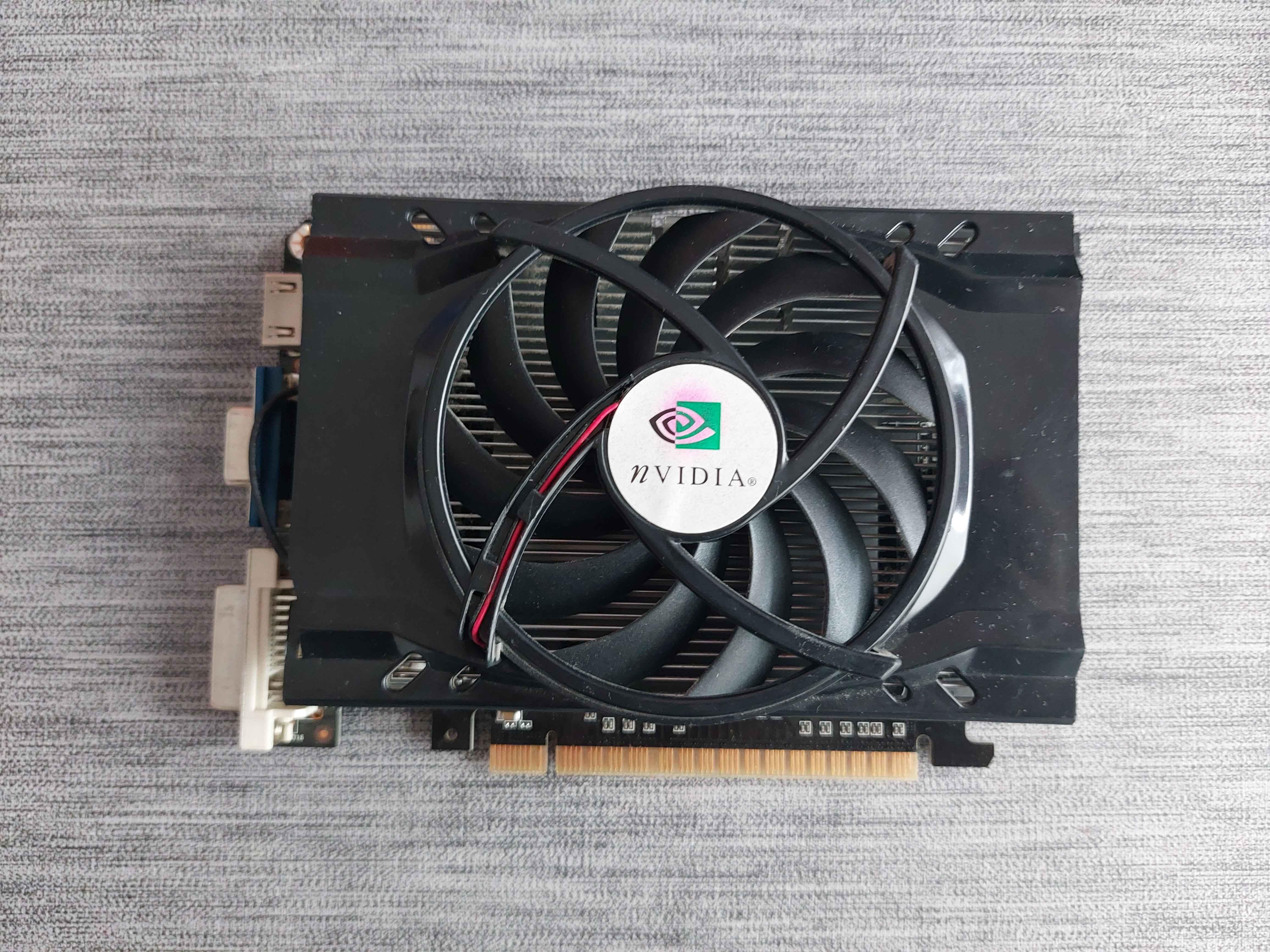 Image 1 of 2 (CircusCat)
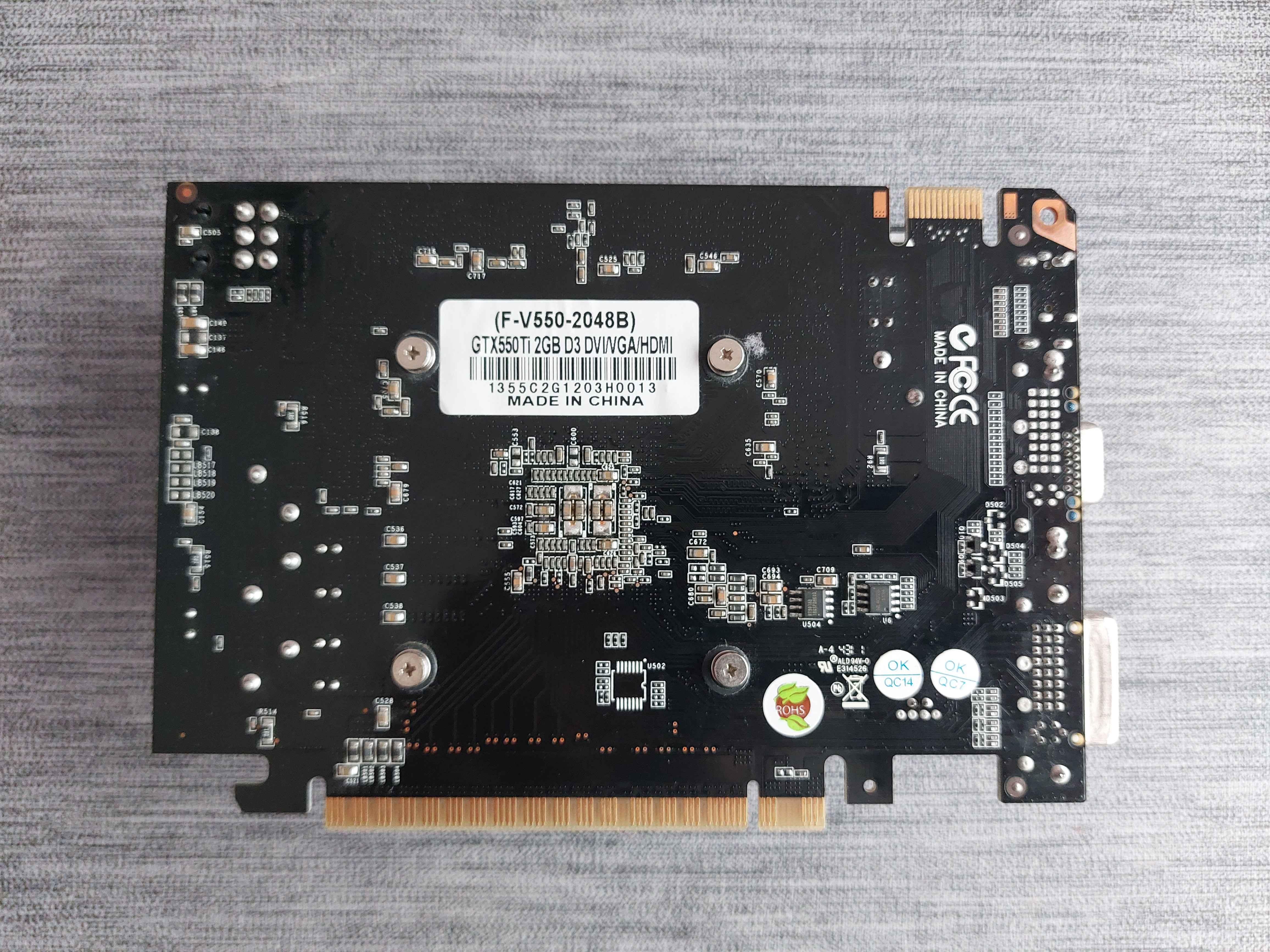 Image 2 of 2 (CircusCat)